
Yamaha Motor Europe Robotics Division – SMT section
Richard Vereijssen B.Sc – Product Marketing manager
Introduction: Miniaturization, Driven By Demand
The global electronics industry’s ability to deliver seemingly limitless ongoing advancements in product capabilities has encouraged an insatiable consumer demand for more, better, and smaller. Demands for high functionality of mobile devices, smart watches, military, medical, audio, and wearable technology continue to drive requirements for miniaturisation.
The advancements being achieved in large-scale CMOS integration, described by Moore’s Law, are among several factors currently aiding relentless gains in functionality, performance and miniaturisation. The fabrication and packaging processes for manufacturing chip-size resistors and capacitors also continue to advance, enabling components to be produced down to sizes in the region of 0.25mm x 0.15mm (0201). Excellent dimensional stability enables these components to be assembled using standard inline surface-mount equipment.
Initially, the tiniest components (not only 0201: adoption of 01005 will begin in the foreseeable future) are expected to be used in extremely space-constrained applications, such as System in Package (SiP) or Package in Package (PiP) devices. These answer demands for extreme miniaturisation and circuit densification in mobile devices, like smartphones and tablets. Ultimately, of course, they will be demanded for general surface-mount assembly in PC motherboards, industrial automation products, IoT nodes and gateways, and others. Automotive electronics is another sector that demands increasing circuit capability and complexity, where small size and lightness are key desires of product designers.
1. Progression of Chip-Component Sizes
Continuous advancements, both in manufacturing capabilities and market demand for smaller or more feature-rich end products, has driven relentless miniaturisation of component sizes generally, manifested in the emergence of semiconductor packages like flip-chip and CSP, power-discrete packages like LGA, and surface-mount chip resistors and capacitors in ever-smaller form factors: as figure 1 shows, the 1005 (1.0mm x 0.5mm) form factor has been the most widely used since the mid 2000s to date, while more recently an increasing number of designs have targeted the smaller 0603 (0.6mm x 0.3mm) size; sometimes even when design space is not a concern. The popularity of 0402 (0.4mm x 0.2mm) devices is currently rising, while 0201 devices are expected to supersede the older 1608 (1.6mm x 0.8mm) form factor around the year 2022.
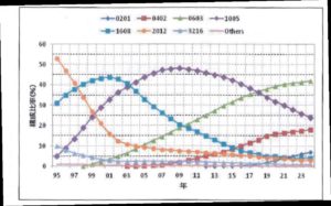
Figure 1. The 0201mm form factor for chip components is expected to become dominant by 2022.
The table compares metric and imperial component designations, with their applicable sizes. Confusion abounds, particularly where designations clash – such as 0603, 0402 and 0201. As the drive continues to explore further miniaturisation, it will be preferred to standardise on metric nomenclature going forward as an aid to communication and to avoid confusion when referencing components.
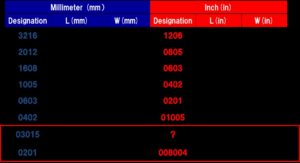
Table 1. Comparison of metric and imperial designations for standard chip components.
Note that only chip resistors – not capacitors – have been offered to the market in the 03015 form factor.
Moreover, two different “0201” outlines have been proposed by various manufacturers: 0.2mm × 0.1mm and 0.25mm × 0.125mm. The industry needs a single commonly accepted standard and, indeed, 0.25mm × 0.125mm is expected to become the accepted specification.
The shock and awe comes when comparing the area and volume of the later, smaller form factors with their predecessors like 1005. The area of an 0201 component, when mounted on the substrate, is 0.0313mm2: only 6% of the area occupied by a 1005-size chip. Moreover, the volume of a 0201 capacitor – typical height 0.125mm – is 0.004mm3, or just 1.6% of the volume of the 1005 parts. 0201 resistors are even lower volume, having thickness of 0.08mm.
The first major deployments of 0201 devices are expected to be in highly integrated package-in-package assemblies, aiming to achieve further circuit-size reductions in products such as smartphones, tablets, and IoT devices.
This paper discusses board design, as well as printing, mounting, and inspection processes for assembling 0201 devices, as the next major challenge for product designers, OEMs and EMS businesses. All need to understand how these components can be adopted in surface-mount assembly processes, achieving the accuracy and repeatability needed to ensure high end of line yield for commercial viability. This calls for an evaluation of the key issues affecting the performance of printing, component mounting, and inspection processes.
The presentation, configuration and materials for tape and reel, at the smaller component sizes, are still being developed. Paper tape is inefficient, in terms of parts per linear millimetre. Although 0201 parts today are usually packaged in W4P1 (4mm width, 1mm pitch) embossed tape, the narrow tape width is difficult to handle, and W4P1 feeders are expensive. A W8P0.5 specification has been proposed.
2. Board Design
Developing an assembly process for any product begins with the PCB design as the foundation for the project; in particular, the pad sizes and positions, and distances to adjacent components.
Previous experience shows that the relationship between the pad size and the aperture size has an important influence on paste release. When the copper is etched, the resulting pad can become slightly smaller than the designed aperture of the stencil. If this happens the paste at the edge of the aperture cannot touch the pad and instead is suspended in the gap between the pad and the stencil. As a result, the paste at the edge of the aperture may fail to release when the stencil and substrate are separated.
Figure 2 shows how detachment defects can occur when the pad is slightly smaller than the aperture. Transfer rates become erratic, resulting in insufficient paste or poorly shaped deposits. To combat this, the pad design will need further work to establish suitable guidelines for pad size, spacing between pads, and distances to adjacent components. One recommendation is to oversize the pad to ensure contact.
Figure 2. Adhesion to the pad near stencil edges is important to ensure proper paste release.
3. Printing
For the print process to be successful, at the smallest chip-component sizes, each element needs to be reviewed and optimised. The bottom line – as always – is that is that if print results are not repeatable, defects are in-built from the start that cannot be remedied by corrections further downstream. Printing is the process that presents the most challenges, particularly in relation to mixing the smallest components with larger components in a high-volume application.
There are mainly four points to consider, to establish a secure and stable printing process:
(1) The seal or gasket between the stencil and PCB
(2) Controlling the aperture fill
(3) The release of the PCB/paste from the stencil
(4) PCB support
As far as paste release is concerned, strong adhesion between the solder paste and the lands on the substrate (usually exposed copper pads on FR4 PCB) is needed to overcome the friction between the solder paste and the aperture walls. This is influenced by board design, as described earlier and in section 3.3, stencil design including aperture surface finish and any low-friction treatment that may be applied (section 3.5), and the stencil/board separation speed selected at printer setup. Solder paste vendors typically recommend a constant separation speed greater than 3mm/s for best paste release and cycle time.
PCB support, or tooling has a key role in the success of printing small feature sizes. The rule of thumb is that the more support, the better the results. The aluminium tooling plate remains the gold standard for support. Experience with double-sided boards containing densely spaced components has shown that grid tooling is superior to pins. However, a tooling plate may be required for substrates less than 1mm thick. Note that top clamps should be avoided, as these can adversely affect aperture filling at distances of more than 25mm from the board edge.
Before discussing changes to the print and placement processes, it is important to mention the cleanliness of the machine. Excess paste accumulating in the printing machine, becoming dry and hard over time, can have obvious negative effects on the print results. As the scope for variation becomes large when dealing with small component printing, it is vital to be sure the results are not impacted by random dropped paste.
3.1 Stencil-to-PCB Seal: Controlling the Gap
Maintaining adequate contact between the stencil and substrate as the squeegee passes over the stencil apertures is important. A good gasket created by proper contact between the PCB and stencil will reduce bleed-out of the paste and help lower stencil-cleaning frequency. Various types of defects may result from an excessive gap between the stencil and substrate.
Before attempting to print with challenging aperture sizes, the machine calibration between the board and the stencil should be checked to make sure it is within the manufacturer’s specification. The PCB thickness should also be measured properly, not using guesswork, and measuring a random sample of the lot to ensure consistency. Improper sizing can either over-drive the PCB into the stencil, or create a gap that will produce poor results.
If the aperture size is small, insufficient paste may come into contact with the pad resulting in a lack of adhesion (figure 3). In this case, paste remains in the stencil apertures instead of transferring to the substrate after separation.
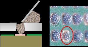
Figure 3. Poor adhesion can prevent paste release upon stencil separation.
On the other hand, a proportion of paste can escape from stencil apertures and spread onto the substrate surface (figure 4). With the smaller apertures for 0201 size components, the process becomes more sensitive to the volume deposited and less tolerant of un-released or escaped paste.
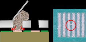
Figure 4. Paste can escape onto the substrate surface, causing defects like bridging.
Vacuum clamping, after alignment and before the squeegee excursion begins, is recommended to ensure accurate positioning and maintain contact between the stencil and substrate throughout the printable area. To ensure accuracy is maintained, after vacuum is applied, the stencil frame must be sufficiently rigid. Recognising that low-cost stencil frames can lack the required rigidity, and may distort when vacuum is applied, these should be carefully considered: upgrading the stencil specification to a frame of higher quality may be necessary.
Under any circumstances, small gaps are likely to occur between the substrate and stencil, and can be tolerated within certain limits. Experimentation has shown that a gap of up to 0.2mm can be tolerated, resulting in acceptable print quality. Figure 5 shows compares the volume of paste transferred to the substrate through 0.22mm x 0.24mm stencil apertures for stencil-substrate gap as large as 1.0mm, demonstrating acceptable repeatability up to about 0.2mm.
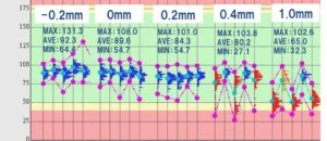
Figure 5. Paste-volume repeatability is acceptable with a stencil-substrate gap of about 0.2mm.
If the maximum acceptable gap is not to be exceeded, it is imperative to ensure the upper surface of the substrate and lower surface of the stencil are extremely clean. Moreover, other features that affect surface flatness – such as labels or silk-screen printing of a board-ID barcode or component-position identifiers – can significantly challenge process control. A typical silk-screen process can produce ink deposits that may be between 20µm and 100µm thick, which is enough to allow unwanted leakage of paste from apertures during printing. Elimination of silk screening for component identification is recommended.
Among potential solutions, Photo-Imageable Embedded Reference Designators (PIERD® – a trademark of Tokai Shinei Electronics Corporation Limited) can create visible markings in the solder-resist layer and require no ink to be deposited on the surface of the substrate. Alternatively, new flexible stencils have been developed, such as the Taiyo Yuden ER type, Nakanuma FIT, Micron Process Lab PH, or Cube SMT Lab P-Cube Stencils. These feature a resin coating on the underside of the stencil, typically between 10µm and 30µm thick, which conforms against small surface irregularities to prevent paste escape.
Another key point is to ensure the PCB solder-mask height is level with the pad height. Sunken pads, at a lower height than the mask, produce a gap that prevents contact between the board and stencil resulting in erratic print deposits.
3.2 Controlling Aperture Fill
Proper filling of the stencil apertures during squeegee excursion is known to depend most strongly on paste pressure and excursion speed . Squeegee pressure has an impact on filling, but reaches a point where the effect on the paste becomes saturated and blade deflection is the result. This tends to cause scooping from larger apertures, resulting in poorer filling.
Paste pressure is related to the weight of the paste roll on the surface of the stencil, and the squeegee angle. Squeegee angle has been shown to have a greater impact on the aperture fill than the conventional parameters of speed and pressure. The ability to optimise the angle between 65 degrees – typically used for low-viscosity materials – and 45 degrees used for polymer or adhesive printing enhances the ability to maximise aperture fill. Reducing the squeegee angle extends the time that the material spends over the aperture. In addition, a greater proportion of the blade surface area is in contact with the material, and so increases the impact on aperture filling.
The optimal range for printing with solder paste is between 60 and 50 degrees. By reducing the squeegee angle as the paste roll size diminishes (as the paste is forced into the stencil apertures), the paste pressure can be kept more or less constant between the times at which the paste is replenished. Some printing machines have no ability to vary the squeegee angle, so the blades are normally set to 60 degrees. As the size of the apertures becomes smaller, with the introduction of 0201 chip-size components in mainstream SMT manufacturing, the ability to vary the squeegee angle – as provided by the Yamaha 3S (Swing Single Squeegee) head – delivers an advantage for process control and consistency.
3.3 Paste Release: Adhesion of Solder Paste and Lands
The industry still needs to establish optimal land sizes for soldering 0201 terminations. The aperture size should be slightly less than the land size, to maximise adhesion at the areas of the land closest to the edges of the aperture and thereby ensure consistently good paste release and deposit shape.
The transfer efficiency of the apertures can be determined using aspect-ratio and area-ratio formulas. The aspect ratio (aperture width ÷ stencil thickness) can show whether the stencil thickness is appropriate for the aperture width, but does not give a clear picture of the transfer efficiency. An aspect ratio of 1.5 is generally recognised as the minimum for acceptable paste release.
The area ratio (bottom area ÷ lateral area) is illustrated in figure 6. This provides a better indicator of transfer efficiency. As component dimensions and solder-terminal sizes have reduced, so too has the minimum acceptable area ratio for stencil apertures. When first introduced, the minimum score was 0.66. For the latest components, an area ratio of about 0.40 is considered mandatory.

Figure 6. Area ratio.
To satisfy either of the formulas, the contact area of the pad must be greater than the total area of the aperture wall. Effectively, the stencil thickness must be reduced to ensure satisfactory paste release at smaller aperture sizes. Figure 7 describes typical stencil thicknesses for the land sizes appropriate to commonly used chip-size passives and surface-mount IC packages. Components as small as 03015 or 0201 need the stencil thickness to be in the range 40µm to 60μm.
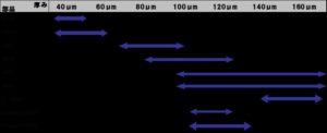
Figure 7. Appropriate stencil thickness, according to component size.
Boards containing a mixture of the smallest and largest components, like connectors or discrete power components, can challenge attempts to identify a suitable, uniform stencil thickness. A thin stencil, needed to print paste for 03015 or 0201 chips, may be unable to deposit the quantity of solder required for the larger parts.
Known solutions to this challenge include selective etching of the stencil, in locations where small components are used, to reduce the thickness and so improve paste release. This can be economical, and is possible to implement without needing to use a special squeegee, such as a flexible non-metallic, squeegee. On the other hand, the board design may be constrained by the fact that the squeegee cannot follow the contours of the stencil if the etched areas are small. The smallest components may need to be confined to a limited area, which may not be practicable.
As an alternative, a thinner stencil of uniform thickness suitable for printing deposits for smaller components can be used, and solder preforms placed on the pads for larger components to ensure enough solder is present for satisfactory reflow. These preforms are placed using conventional mounting techniques, but add to the BOM cost for the board and can significantly extend the cycle time for the mounter.
In addition, stencils below 50µm thickness can be expensive, fragile, and difficult to procure. Greater susceptibility to “coining” caused by repeated contact of the PCB and squeegees can also shorten the operating lifespan.
3.4. Sequential Printing to Cover the Full Component Range
Sequential printing can offer an effective alternative. In this approach, two stencils of different thicknesses are used – one after the other – to apply paste to the same substrate. This enables two different grades of solder paste to be deposited, and gives extra freedom to position small components anywhere on the board, without recourse to placing preforms on pads that require a larger volume of paste. A dual-lane printer with a sequential printing mode, such as the Yamaha YSP20, is needed. Figure 8 shows the results of sequential printing, using separate stencils for 1608 and 03015 components respectively.
Sequential printing also provides the opportunity to reduce the cost of solder paste deposited on the board, by using the more expensive type 5.5 or 6 paste for printing fine features only. A coarser particle size can be used for depositing larger volumes of paste.
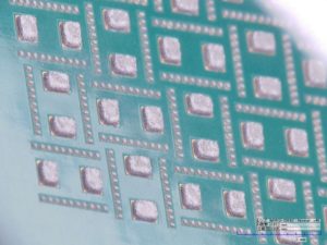
Figure 8. Sequential printing using stencils of different thickness allows the print process to handle a large difference between the solder volume required for ultra-small components and that needed for larger devices.
3.5 Stencil Treatments for Improved Paste Release
The surface roughness of the aperture walls is known to be an important factor influencing paste release. A low-friction surface is desirable, but applying extra polishing or coating processes to the stencil at manufacture adds to cost.
Laser-cut stencils can be subjected to electrolytic polishing, which is more effective than physical polishing, in terms of its effect on the inner surfaces of the apertures. Physical polishing is effective in removing burrs from the aperture edges, which can aid sealing at the stencil-substrate join, but has little if any effect on surface finish inside the aperture.
Electrolytic polishing ensures a smoother surface, and a further water-repellent silicone-based coating process can be applied to ensure the lowest possible friction.
Alternatively, additive (electro-formed) stencils are known to benefit from aperture walls that have inherently lower surface friction than laser-cut apertures. Bearing in mind that the reduced stencil thickness needed to print deposits for 0201 components has the effect of lowering demands on the additive process – in terms of material deposited and time to complete the process – the cost premium for electro-forming can be lower compared to a laser-cut stencil.
However, additive stencils can display variable stencil thickness, across the surface of the board, with inaccuracy and encroachment of the aperture size, during the additive process. Image stretch introducing during the photoresist phase can also be an issue. On the other hand, the accuracy of laser-cutting processes, combined with today’s high-quality fine-grain steels that produce smooth aperture walls, ensure laser-cut stencils remain a popular, effective and economical choice.
3.6. Experimental Study of Aperture Size, Stencil Properties and Solder Paste
Yamaha has analysed printing processes for 0201 components, comparing performance with various aperture sizes, solder paste types, and stencil manufacturing techniques.
The experimental conditions are as follows:
Solder pastes:
① Senju Metal Industry M705-RGS800 Type 5 (average particle size 20μm)
② Senju Metal Industry M705-RGS800 Type 5.5 (average particle size 15μm)
③ Senju Metal Industry M705-RGS800 Type 6 (average particle size 10μm)
Stencils (each thickness 50µm):
① Sonocom laser + electrolytic polished
② Sonocom laser + electrolytic polished + liquid-repellent coating
③ Sonocom additive + liquid-repellent coating
Printer setup:
Model: YSP with 3S squeegee
Stencil detach speed: 3mm/sec
Squeegee angle: 55°,
Squeegee speed: 50mm/sec
Squeegee pressure: 60N
Solder print inspection:
Model: YSi-SP high-resolution type (5/10μm)
(measure solder volume fraction with 10 consecutive sheets)
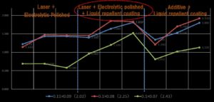
Figure 9. Process capability comparison for aperture sizes, solder paste types and stencil properties.
Figure 9 shows the calculated process capability for each combination of aperture size, solder paste and stencil type. Several conclusions can be drawn:
• Laser-cut and electro-polished stencils with water-repellent coating are able to support 0201 processes, and can deliver results superior to the additive-formed stencil
• The water-repellent coating significantly improves the laser-cut stencil performance
• Type 5.5 solder paste can deliver comparable results to more expensive type 6 pastes. Type 5 paste shows inferior performance
A Note on Solder-Paste Particle Size
The successive reductions in SMD chip-component sizes, and the effects on aperture designs, have pushed paste requirements towards finer particle sizes (table 2).
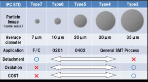
Table 2. Standard paste types and suitable applications.
The transition from Type 3 paste, with 35µm typical particle size, to 30µm Type 4 pastes was driven not only by the promise of greater end of line yield but also by reductions in the cost of Type-4 pastes due to rising demand. A similar transition is occurring in the present timeframe, as the cost of Type-5 pastes is becoming lower with increasing adoption in high-volume manufacturing processes.
The arrival of 0201 on factory floors is pushing the requirement to Type-6. The current high price of Type-6 pastes reflects today’s low-volume applications for 0201 components in semiconductor and specialised applications. Whereas the Type-5 powder costs about 40% compared to Type-4, the material cost for Type-6 pastes can almost triple. This is of concern to high-volume manufacturers.
Looking at the average particle sizes from Type-3 to Type-7, in Table 1, there is a significant difference between Type-5 and Type-6, where the ball size is reduced by half from 20µm to 10µm. Noting that paste suppliers have offset the premium for Type-5 pastes through a blend of powder sizes that create a Type-4.5, the opportunity exists to create a Type-5.5 with average particle size of 15µm. This could address the cost concerns, and may also reduce the risks associated with oxidation of the smaller particles and challenges associated with reflow. The experimental study compared results for Type-5, Type-5.54 and Type-6 pastes to assess the impact of particle size on process performance.
4. Optimising the Mounting Process for 0201 Components
Assembling ultra-small components down to 0201 size (and even smaller in the future), also challenges aspects of the mounting process. Accurate component pickup holds the key to satisfactory placement, and is dependent on correct alignment of the nozzle and feeder, as well as correct pickup height.
When picking up small chip resistors or capacitors, there is minimal tolerance for any offset between the centre of the component and the centre of the nozzle. In addition to errors in feeder and nozzle position, other factors such as temperature difference also have increasing influence over the placement accuracy of smaller components.
Automatic correction, using a system such as Yamaha’s Multiple Accuracy Compensation System (MACS) compensates for all sources of error in the machine’s mechanisms. MACS helps to ensure component pickup at the nozzle centre by identifying the centre of the component as it is presented in the feeder tape, and by recognising the image of the nozzle tip to automatically correct for deviation from the theoretical centre. MACS has been shown to improve accuracy by a factor of three, reducing positional errors to less than 10µm (3 sigma).
Automatic pickup height teaching is also critical, both to prevent damage to the small and delicate components, and to prevent mis-orientation of the component after applying the positional corrections calculated by MACS.
Figure 10 illustrates aspects of the mounting process that can affect placement accuracy, and the elements that are addressed using auto position compensation and pickup-height teach.

Figure 10. Automatic calculation of pickup height and nozzle position, with accuracy compensation.
A note on Nozzle Maintenance
The appropriate nozzle for picking up 0201 components has a pore size of 0.1mm. This extremely small pore size is more vulnerable to blocking by tiny particles than larger nozzles such as those used for 0603 or larger components. Cleanliness, therefore, is of the essence, and frequent nozzle cleaning is recommended. Automatic cleaning of all nozzles simultaneously, using a cleaner such as the SAWA Nozzle Cleaning Unit with built-in ultrasonic cleaning, can be effective and efficient. After cleaning, the entire bank of nozzles is reinstalled and aligned in a single operation.
5. Inspection
Commonly used inline automatic optical inspection (AOI) systems tend to contain a 5-Mpixel sensor and cover a field of view that gives image resolution of about 19 μm. When inspecting 0201-size components, this is not sufficient to provide a crisp, clear image that can be analysed easily and accurately.
To increase the resolution, the field of view must be reduced if the 5-Mpixel sensor is to be retained. One drawback is that extra images must be captured to cover the entire board, resulting in longer cycle times.
On the other hand, more advanced cameras with 12.58Mpixels are now available. These can allow high-speed, high-precision inspection with selectable resolution of 12μm or 7μm, and a large field of view.
The advantages of using the latest high-resolution cameras can be additionally boosted by also applying multi-dimensional and multi-angle inspection. Yamaha’s YSi-V series is capable of 3D and 2D visual inspection, at each of four different angles and in red, blue and green wavelengths, to give a multi-direction view of each component. In addition, there is laser checking for coplanarity and component-height. Users can select from various imaging and detection methods, depending on the requirements of each individual application.
Conclusion
The latest ultra-small components are here to stay, and make printing and placement even tougher. Manufacturers must respond by understanding the most effective techniques and equipment to solve the challenges and using these to perfect new processes.
Superior control over squeegee angle, stencil thickness, alignment of mounter feeders and nozzles, pickup height, and versatile inspection modes including multi-angle, multi-wavelength, and high-resolution cameras support the advanced capabilities needed. Stencil characteristics, including rigidness of the frame, electrolytic polishing, aperture coatings, and conformable stencils that compensate for the effects of silk screening on the substrate, are also more critical.
The findings presented in this paper can help all manufacturing businesses to achieve satisfactory process capability with minor changes to equipment and materials.
To speak to a Yamaha technical specialist about developing processes for the 0201 generation and beyond, please call your local sales office, email, or see the website.
ABOUT YAMAHA Robotics FA Section
Yamaha Factory Automation Section (FA Section), a subdivision of Yamaha Motor Robotics Business Unit in Yamaha Motor Corporation, is focused on delivering flexible, high-accuracy industrial robots for precision automation challenges.
With its roots in the introduction of robot technology to Yamaha motorcycle assembly activities, the division has over 40 years’ experience solving automation challenges from factory-scale to micron-level. Yamaha’s industrial robots are now trusted by leading corporations worldwide, in activities as diverse as semiconductor fabrication and assembling electronic products, domestic appliances, automotive components, and large liquid-crystal panels.
Yamaha Motor FA Section offers a unified range of solutions for robotic assembly, including single-axis robots, SCARA, cartesian, and articulated robots. Innovations such as the LCMR200 linear conveyor module; a smoother, space-saving and more versatile successor to conventional belt and roller conveyors continue to set the pace in factory automation. Core robotic technologies as well as key components and complete robot systems are all produced in-house, ensuring consistent quality and control over lead-times.
Headquartered in Neuss, Germany, Yamaha FA Section serves customers in all Europe.
https://fa.yamaha-motor-robotics.de/
#DiscoverYamahaRobotics